Contents
 CMTC Platform: 40 Years of Innovation to advance the Characterization of Materials
 Material sciences: new trends and expectations for haracterization
 Using tomography to see inside an object
 Electron microscopy: a variety of complementary techniques
 ASTAR: a revolutionary TEM system developed by Grenoble INP
 X-ray diffraction to analyze crystalline materials
 CMTC: enabling and improving the work of an industrial
 Training for material characterization at Grenoble INP
 Glossary
 CMTC Platform: 40 Years of Innovation to Advance the Characterization of Materials
 Grenoble INP once again distinguished itself as the leading French university in the field of material sciences. It was recognized in the QS University Rankings for engineering, where it is the only French institution to be in the top 100 worldwide. The school’s expertise in material sciences is in large part due to numerous cutting-edge characterization techniques, which enable scientists to study and understand a material’s structure and properties at the smallest of scales.
 The CMTC (Consortium of Shared Technological Equipment) platform has been at the heart of Grenoble INP’s capacity to characterize materials. Created in 1997, the CMTC was an innovative approach to mutualize essential scientific equipment. The platform was launched under the leadership of René Molins, who directed the CMTC from 1978 to 1994. The platform currently counts 15 mid-sized characterization tools along with experts that are specialized in each technique.
Over the past 40 years, the platform’s technological offer has diversified to meet constantly evolving needs. Scientists can now benefit from a wide range of tools and techniques available at the CMTC and major research facilities (ESRF, ILL, etc.). This allows them to visualize materials and understand their structure and chemical composition at various scales.
Several trends have defined the evolution of characterization equipment. First and foremost has been the race to reach the smallest scale. Scientists can now observe and characterize materials at a millimetric scale and down to the atomic level. More recently, the need to visualize a material’s volume has led to the development of 3D characterization techniques such as tomography. The final trend has been to develop in-situ characterization, which enables scientists to observe a material while it is being used.
Laurent Maniguet
Director of the CMTC
Material sciences: new trends and expectations for characterization
One definition of the term “material” is to consider it as matter with a function. This definition has guided the development of material sciences. The trend has been to develop customized materials that have multiple functions. They are created using a combination of materials, shapes and scales that have given rise to new material functions and characteristics. These materials are also being developed to be more efficient, sustainable and recyclable.
This guiding trend has forced material characterization experts to explore new constraints and conditions. These multi-functional materials require scientists to focus on material interfaces and very precise measurements of local characteristics and structures. Materials that include targeted chemical components require the use of metallurgy techniques that are a challenge in terms of characterization. The need for sustainability has encouraged the development of controlled characterization in-situ, while the need for recycling has created renewed interest in analytical chemistry.
Grenoble is particularly well positioned to overcome these challenges. Our ecosystem is a leader in terms of architectured materials (Labex CEMAM). We can take advantage of the CMTC as well as major European research equipment (ILL, ESRF, etc.). The CMTC has dedicated the past 40 years to the acquisition and use of the most advanced characterization tools. The platform has always worked to balance research, training and collaboration with industry. It serves as an excellent example of dynamic collaboration and mutualized equipment. In addition, the platform’s capacities are complementary to our ecosystem’s major research facilities.
To continue developing customized materials, we will have to evolve beyond traditional materials. New materials will be multi-functional in order to reduce quantities. To achieve this goal, they will be created using a variety of materials and architectures. They will have to be designed to favor sustainability and recycling. This change translates to a change in paradigm for characterization that can be summarized as “local, environmentally friendly and multi-scale.” The challenge leaves the CMTC with fascinating work for its next 40 years!
 Yves Brechet
Grenoble INP professor and member of the French Academy of Sciences
Using tomography to see inside an object
Radiography, from which is derived tomography, enables scientist to look inside objects using X-rays. Tomography allows researchers to see variations in thickness or density and discover imperfections such as internal cracks.
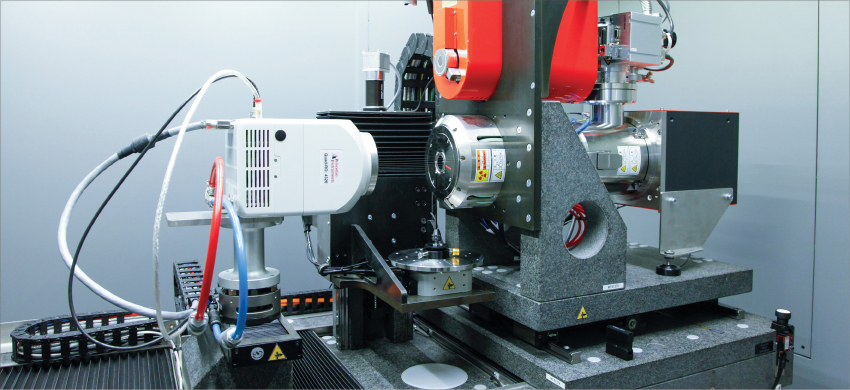
The SIMAP uses this technique to study the solidification and deformation of material in situ. “These real-time observations are carried out at the ESRF because they require fast image acquisition. Usually, one second per 3D image”. As part of research carried out in partnership with the Constellium R&D platform (a platform specialized in aluminum products for aeronautics), this technique is used to study the mechanisms that govern how porosity changes when sheet metal is flattened.
In some cases, an X-ray beam can be replaced by a neutron beam, which is more sensitive to density variations for lighter matter such as hydrogen. The neutrons are absorbed by water and therefore very useful to detect water within various structures.
Pereniti analyzes cement
As part of the Pereniti* chair, Edward Andò, a CNRS research engineer at 3SR, uses this technique to determine how fluids drain through cement tubes used for dams and nuclear confinement. These types of sites are pressurized every ten years to check for possible leaks. “Over time, such structures can developed defects. We have to know how and where. We artificially age cement in order to better understand the degradation mechanisms at play. For example, we can put them through temperature cycles or test them with mechanical forces to check their resistance and impermeability. At the same time, we test solutions to improve resistance by adding aggregates via glue injections”.
A Hassler cell made of titanium was designed and built in 2016 as part of the project in order to carry out cement aging tests and observe high pressure water flows (500 atmospheres). These tests were carried out at the Institut Laue Langevin and enabled researchers to create the world’s first visualization of permeability within such a sample !
*This chair is a partnership between the Grenoble INP Foundation and the EDF engineering centers DTG, CIH and SEPTEN. Frédéric Dufour is the chairholder.
Electron microscopy: a variety of complementary techniques
Electron microscopy includes a variety of techniques such as Scanning Electron Microscopy (SEM) and Transmission Electron Microscopy (TEM). In each of these techniques, an electron beam is directed at the sample in order to capture an image. However, TEM and SEM provide different kinds of data and can be useful for different applications.
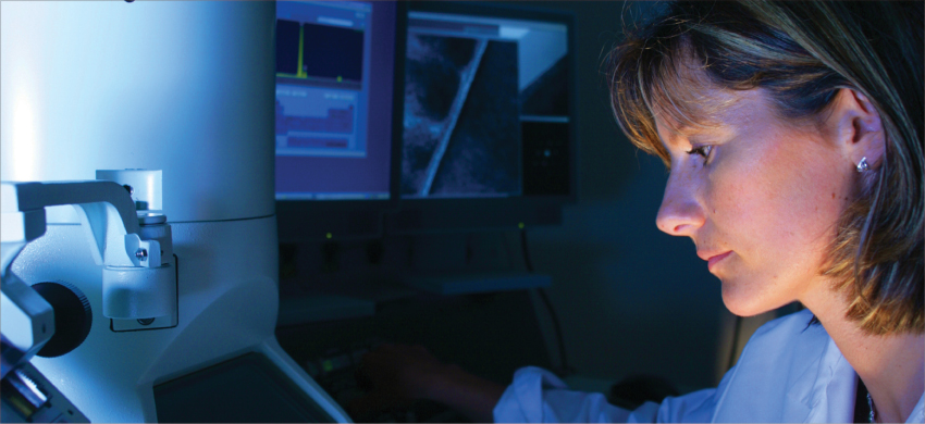
SEM enables researchers to visualize the surface of a sample from which electrons are reflected. In contrast, TEM detects which electrons pass through a sample. In the latter case, the sample must be extremely thin. If it is not thin enough, the sample will be prepared by thinning it down to approximately 100 nanometers. TEM enables scientists to see inside a sample thanks to an almost atomic-scale high resolution image.
TEM produces images that are a far cry away from what one would imagine to illustrated by a super microscope. TEM images can even seem rather vague. However, when analyzed using theoretical understanding, they are rich in information. Much research is in fact aimed at improving the analysis of images and creating tools that facilitate data extraction.
Thanks to additional techniques, it is also possible to visualize a sample in situ, or in other words, while it is functioning. “This ability can be very useful when you’re trying to understand how defects spread across a metal alloy. By understanding these mechanisms, we can imagine how to prevent such defects and thus produce stronger alloys”. explains a researcher at SIMAP. This topic of research is part of a collaborative project between the SIMAP laboratory and industrials such as Arcelor, Constellium and other aeronautical companies.
Laetitia Dubau, a researcher at the LEPMI, also used this technique to study the aging mechanisms in electrolyzers for fuel cells. “We observed the evolution of bi-metal particles of platinum-cobalt and platinum-nickel, which are used as catalyzers for such fuel cells. The images captured using TEM clearly demonstrate that the particles have a tendency to accumulate and the metal added to the platinum tends to disappear during the operation”. These observations enabled researchers to suggest and validate other strategies to improve efficiency.
SEM is also a powerful tool as it allows users to characterize samples at a nanoscale. It can be used for a wide variety of applications. “SEM is very useful for material sciences, whether it’s to learn about the surface of an object or its morphology”. explains Frédéric Charlot, a research engineer at the CMTC. “It also allows us to determine the chemical composition of samples when its is used in combination with chemical analysis techniques and a dedicated detector. At CMTC, we use it to study metals, ceramic materials, microscopy materials and hydrated biological samples”.
The CMTC platform welcomes many researchers and companies to use its scanning electron microscopes. The platform recently acquired a Field Emission Gun (FEG) SEM thanks to the support of the CEMAM Labex. This new tool enables scientists to observe materials at a resolution of 0.6 nanometers The tool can be equipped with additional equipment to learn further information about a sample's mechanical properties*.
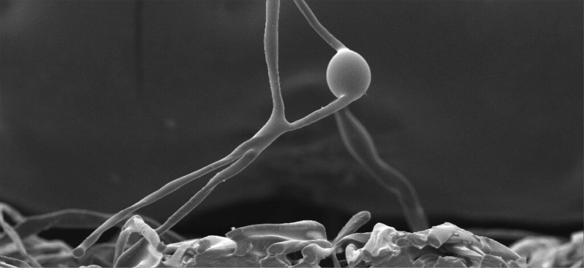
At the LGP2, Raphaël Passas uses these techniques and others** to carry out in situ characterization of cellulose fibers as part of the European PowerBonds project. The goal is to increase bonding between fibers by developing chemical or mechanical modifications that will create lighter paper than what currently exists on the market. The idea is to reduce the environmental impact of paper as well as reduce production and transportation costs.
* in-situ SEM integration tool and local defect analysis tool funded by Grenoble INP AGIR
** Used a micro-robot for fiber flexion and compression funded by Grenoble INP BQR
ASTAR: a revolutionary TEM system developed by Grenoble INP
ASTAR is an ACOM-TEM tool develop by Edgar Rauch, a CNRS researcher, and Muriel Véron, a professor at Grenoble INP. Both researchers work at the SIMAP. Their tool was brought to market in 2009 by NanoMEGAS, an SME specialized in scientific equipment. ASTAR is a patented system that generates and analyzes precession diffraction. Thanks to the tool’s ability to reduce and pivot the beam, it is able to obtain a sample image point by point. “All sample data is collected and stored in order to be analyzed later on by powerful software. The tool provides researchers with more information, a variety of perspectives and faster results”. says Edgar Rauch. By increasing signal quality, this tool creates phase and orientation maps at a nanoscale. It enables users to identify precipitates and distinguish crystalline and amorphous components. It uses a strategy that compares pre-calculated diffraction diagrams to the experimental results collected in situ. The tool uses a dedicated high resolution camera (HRTEM) with Fourier transformation. “This technique is the only one that provides researchers with access to useful structural information for applications such as microelectronics” adds Muriel Véron. “Without ASTAR, images do not have contrast and cannot provide grain orientation”. Approximately 100 ASTAR tools have already been sold and installed around the world.
X-ray diffraction to analyze crystalline materials
X-ray diffraction provides data about a material’s atomic level structure. This is essential to understand both physical and mechanical properties. When a crystal is analyzed with an x-ray beam whose wavelength is similar to the inter-atom distance, the crystal’s atoms communicate a wave that can be used to understand its crystal structure.
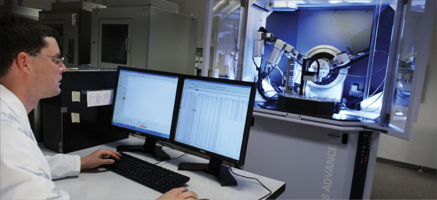
This technique is particularly useful to identify a material’s crystallographic phases. For example, zirconium exists in several crystal forms that have very different properties. “Its monoclinic structure is stable at room temperature, but does not provide enough insulation. Yet this insulating property is that reason why zirconium is useful for microelectronics. This property can be found in its cubique or quadratic structural form” says Stéphane Coindeau, a CNRS engineer at SIMAP. “By adding yttrium or by using processes that create nanometric films, we can stabilize zirconium in its cubic or quadratic structure. X-ray diffraction helps us check and understand the differences between these different structures”. In some cases, this technique can be combine with other techniques such as Raman spectroscopy or X-ray fluorescence.
Hubert Renevier, a Grenoble INP professor at the LMGP, uses the SOLEIL synchrotron and the ESRF to visualize in situ the growth of ultra-thin films (1nm) of ZnO oxides on InGaAs, which is deposited by CVD in a reactor they developed. “These in situ observations allow us to better understand the synthesis of ZnO right when the deposit process begins”.
CMTC: enabling and improving the work of an industrial partner
UP-SGI has a location in Seyssinet where the majority of its turnover is earned by maintaining equipment for the microelectronics industry. The company provides services to clean reactors used to produce components with chemical or physical deposits (PVD and CVD). “When various thin layers are deposited on silicon substrates, these materials are also deposited on the chamber walls inside the reactor. Over time, these deposits accumulate and can contaminate the chip production process” explains Olivier Marchand, head of European R&D at UP-SGI.
To decontaminate these chambers, UP-SGI uses several techniques such as high temperature chemical processes or mechanical abrasion techniques. Once the accumulated deposits have been removed, the company also offers to cover the chamber surface with protective coatings that help limit impurities and improve equipment performance.
To guarantee the efficiency of these coatings, Olivier Marchand relies on advanced microscopy techniques. As a result, the company often calls upon the CMTC’s expertise and equipment. “We regularly use the CMTC platform to analyze our samples, improve our techniques and characterize defective equipment”. UP-SGI even participated in the CMTC’s acquisition of a new FEG-SEM, which will be installed later this year with the support of Grenoble INP.
Training for material characterization at Grenoble INP
The study, design and characterization of innovative materials for transportation, energy, leisure activities, healthcare, microelectronics and construction represents an important educational focus at Grenoble INP- Phelma. Phelma offers numerous options for students in Engineering and Master’s programs (e.g., Material Sciences and Engineering program, or international training programs such as the master’s in Functionalized Advanced Materials Engineering).
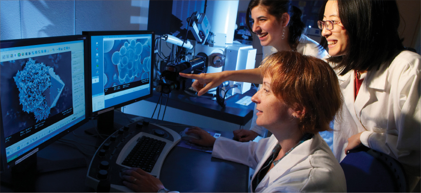
Students in Phelma’s material sciences programs are able to work in research laboratories at SIMAP or with platforms such as the CMTC. As a result, Grenoble INP - Phelma also participated in the purchase of the CMTC’s new FEG-SEM.
The CMTC provides hands on material characterization for Grenoble INP - Phelma students in the Material Sciences and Engineering program (SIM).
By working in groups of four or five, student engineers are able to try out characterization tools and explore material structures. They can discover techniques such as:
• X-ray diffraction at the CMTC (75 students this year)
• Scanning electron microscopy at the CMTC (75 students this year)
• Transmission electron microscopy at SIMAP (38 students this year)
As part of their Reverse Engineering projects, second year students in the SIM program take part in a workshop led by Georges Kapelski, a researcher and professor at Grenoble INP - Phelma and SIMAP. The students get to use the CMTC’s SEMs,including the new Phenom SEM
As part of their Damage Analysis projects, several groups of third year students in the SIM program were also able to use CMTC equipment under the supervision of Alexis Deschamps, a researcher and professor at Grenoble INP - Phelma and SIMAP.
Continuing education also finds it place at the CMTC
Since its creation in 1980, the CMTC microscopy program has trained more than 1,500 microscopy users in France. This program has since been expanded to include other techniques, often in collaboration with other institutions in Grenoble. The latest technique to be offered for training is the “X- ray characterization of thin layers” program, which is delivered in partnership with the INSTN and CEA in Grenoble.
Grenoble INP’s continuing education department currently offers specialized programs that combine theory and hands on practice to learn a variety of techniques. These programs are designed for researchers, engineers and lab technicians. Examples of programs include:
• Scanning Electron Microscopy and X-Ray Microanalysis
• Transmission Electron Microscopy
• X- Ray Characterization of Thin Layers
• Fundamentals of Raman Imagery and Spectroscopy
Glossary
CMTC: Consortium of Shared Technological Equipment
ESRF: European Synchrotron Radiation Facility
ILL: Institut Laue-Langevin
INSTN: French National Institute for Nuclear Sciences and Techniques
Labex CEMAM: Center of Excellence for Advanced and Architectured Multi-Functional Material
LEPMI: Electrochemistry and Physical-chemistry of Materials and Interfaces
LGP2: Laboratory for Paper Engineering and Processes
LMGP: Laboratory for Physics and Materials Engineering
SIMAP: Sciences and Engineering for Materials and Processes
3SR: Laboratory for Grounds, Solids and Structures - Risk


